Take a look at our newest merchandise
![[Windows 11 Pro]HP 15 15.6″ FHD Business Laptop Computer, Quad Core Intel i5-1135G7 (Beats i7-1065G7), 16GB RAM, 512GB PCIe SSD, Numeric Keypad, Wi-Fi 6, Bluetooth 4.2, Type-C, Webcam, HDMI, w/Battery](https://m.media-amazon.com/images/I/71LYTzK2A8L._AC_SL1500_.jpg)


| NVIDIA GeForce RTX 5070 Founders Version: MSRP $549 The ultimate member of the preliminary GeForce RTX 50 sequence launches at this time, the mid-range GeForce RTX 5070, and we have got the total scoop with copius benchmarks and overclocking information.
|
|||

|


|
||
NVIDIA is launching the ultimate member of the preliminary batch GeForce RTX 50 sequence playing cards at this time, the GeForce RTX 5070. First introduced at CES in early July, the GeForce RTX 5070 would be the most inexpensive Blackwell-based GPU in the meanwhile, or at the least till NVIDIA releases data concerning potential GeForce RTX 5060 and RTX 5050 class merchandise.
NVIDIA CEO Jensen Huang famously proclaimed the GeForce RTX 5070 was ‘sooner than a 4090’ throughout his keynote at CES, however as most of you realize by now, that assertion requires some qualification. By way of pure raster efficiency, the GeForce RTX 5070 represents an analogous improve over the older RTX 4070, that its higher-end siblings supply over their previous-gen counterparts. Think about DLSS 4 multi-frame generations, nonetheless, and the GeForce RTX 5070 can easy out in-game animation at a a lot larger charge.
Alas, we’re getting forward of ourselves. Let’s get to know the GeForce RTX 5070 Founders Version, earlier than we dive into some benchmarks. On with it…
NVIDIA GeForce RTX 5070 Founders Version Specs
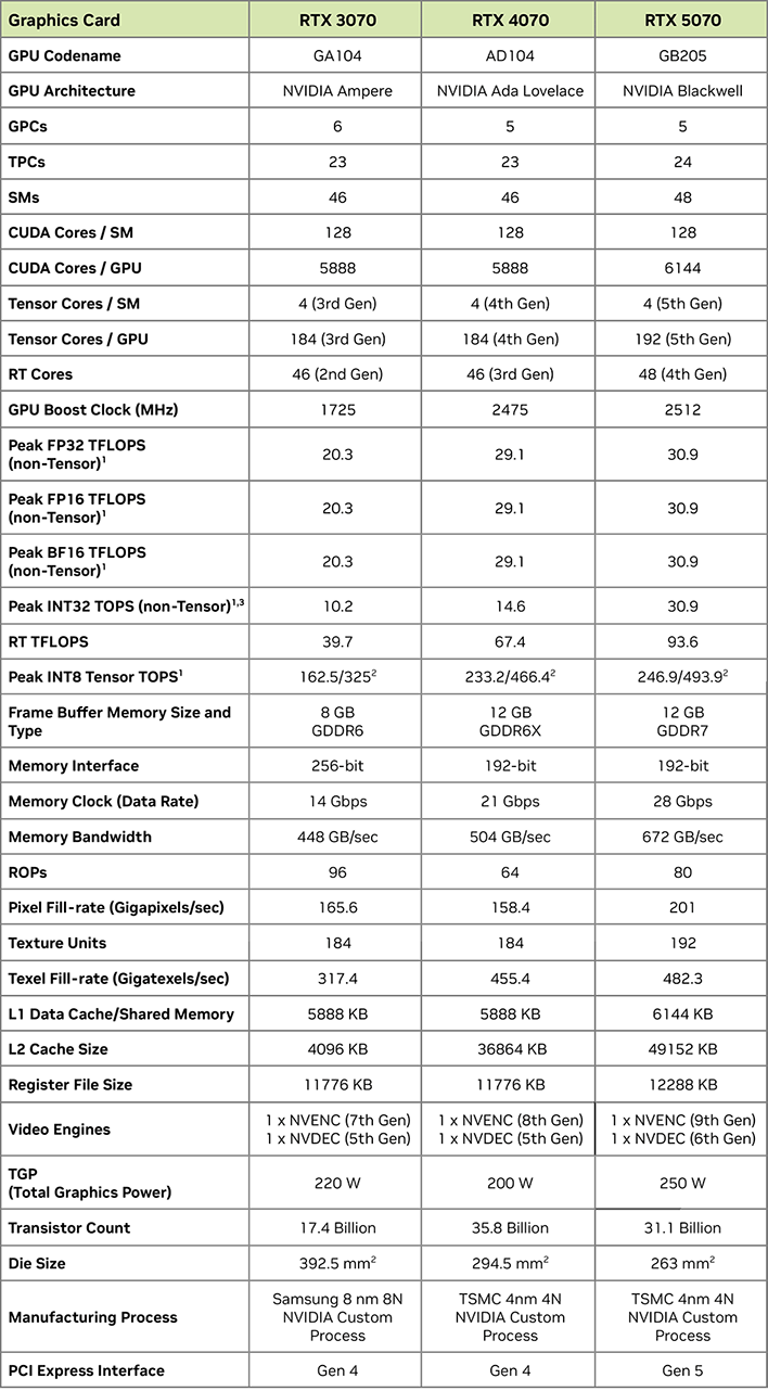
The GeForce RTX 5070 is predicated on one more GPU in NVIDIA’s Blackwell-based portfolio, the GB205. If you happen to recall, the GeForce RTX 5070 Ti and RTX 5080 are based mostly on the bigger GB203, and the flagship GeForce RTX 5090 on the larger-still GB202.
In its fully-enabled type, the GB205 GPU options 5 GPCs, 25 TPCs, 50 SMs, and 6 32-bit reminiscence controllers, for an combination 192-bit reminiscence interface. Tunneling slightly deeper, the GB203 packs a complete of 6,400 CUDA Cores, 50 RT Cores, 200 Tensor Cores, 200 Texture Items, and 80 ROPS. And its cache configuration consists of 6,400KB L1 Cache, a 12,800KB Register File, and 49,152KB of L2 Cache.
All instructed, the chip is comprised of roughly 31B transistors and it’s the smallest xx70-class GPU in a number of generations at solely 263mm2, regardless of being manufactured on the identical course of because the previous-gen AD203.
The GeForce RTX 5070, nonetheless, doesn’t function a full implementation of the GB203. On the GeForce RTX 5070, one TPC and two SMs are disabled, which brings the core counts right down to the 6,144 (CUDA), 48 (RT) and 192 (Tensor), and the L1 and register file down to six,144KB and 12,288KB, respectively.
The GB203 on the RTX 5070 is linked to 12GB of GDDR7 reminiscence working at a speedy 28Gbps, for peak reminiscence bandwidth within the 672GB/s vary, and it options considered one of NVIDIA’s newest encoders and decoders. And complete board energy is rated for 250 watts.
When in comparison with the final couple of generations of xx70-class GPU, the GeForce RTX 5070 is an across-the-board improve in each class. We’ll learn the way all of these specs translate within the real-world quickly sufficient, however we also needs to remind you that Blackwell introduces a number of updates and new options as effectively. You possibly can learn extra about them in our preliminary structure protection, right here.
Checking Out The NVIDIA GeForce RTX 5070 FE
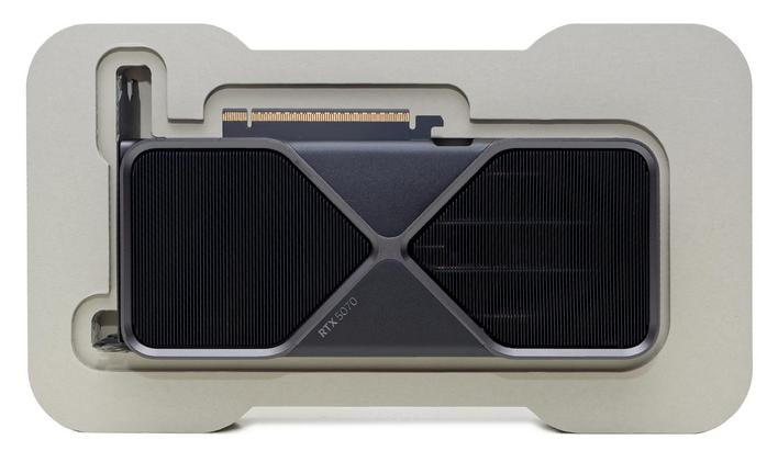
The GeForce RTX 5070’s industrial design and general aesthetics, resemble the higher-end GeForce RTX 5080 and 5090 Founders Version playing cards, however the RTX 5070 is considerably smaller and extra compact.
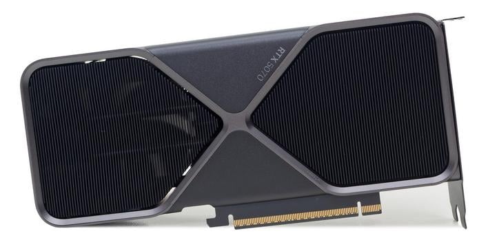
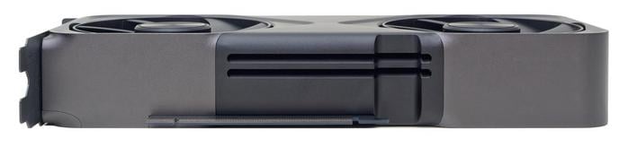
The cardboard measures solely 9.5” lengthy, two-slots extensive, and about 4.5” excessive – the shroud is barely larger than the case bracket. It is a dense bundle that makes use of premium supplies thoughout, and presents as a “mini-5090”.
In contrast to its bigger siblings, the GeForce RTX 5070 doesn’t function a “Double Circulate Via” cooler design, which permits each cooling followers to blow air straight by way of the heatsink. It’s a Single Circulate by way of design, just like the previous-gen GeForce RTX 4070. NVIDIA’s newly designed cooling options on the RTX 50 sequence playing cards, nonetheless, are extra succesful than previous-gen choices, whereas additionally emitting much less noise.
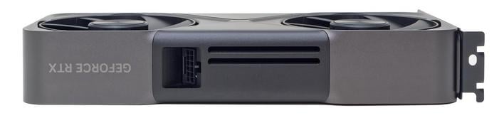
On the prime of the cardboard, you may discover the acquainted 12VHPWR 16-pin connector, additionally used on the RTX 40 sequence. On the RTX 5070 although, the connector is angled off the again on the PCB, and recessed barely within the shroud. This configuration ought to enable for simpler cable administration and reduce the necessity to bend the facility feed in thinner PC circumstances. The included energy adapter requires two PCIe 8-pin feeds, however the cabling is longer and much more versatile than the adapters included in older RTX 40-series playing cards. The connector on the adapter can also be beefier and emits a strong “click on” when pushed totally into place.
The GeForce RTX 5070 incorporates a chilly plate, with a dense array of heatsink thin-fins, linked by way of warmth pipes, just like the RTX 5080’s – simply smaller. NVIDIA additionally makes use of a extra conventional phase-change TIM on the RTX 5070, so not one of the complexities related to liquid metallic are at play.
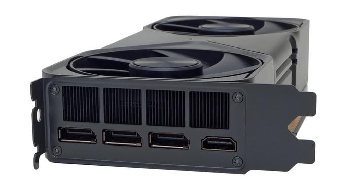
Outputs within the GeForce RTX 5070 (and different RTX 50 sequence playing cards) embrace a trio of DisplayPorts (2.1b) and a single HDMI port (2.1b). Their orientations have been reversed versus previous-gen playing cards although, and the case bracket incorporates a strong entrance bezel with an anti-fingerprint coating.
And with that you have gotten a tour of the GeForce RTX 5070 Founders Version’s design, so let’s get to some benchmarks…
![[UPDATED 2.0] Phone mount and holder compatible with Samsung Z Fold 2 3 4 5 6 Pixel Fold or Foldable phone | bicycle, treadmill, handlebar, elliptical, stroller, rail, handle, roundbar, golf cart](https://m.media-amazon.com/images/I/51CjGlidGRL._SL1023_.jpg)